- 您现在的位置:买卖IC网 > Sheet目录3882 > PIC16F87T-E/SS (Microchip Technology)IC MCU FLASH 4KX14 EEPROM 20SSOP
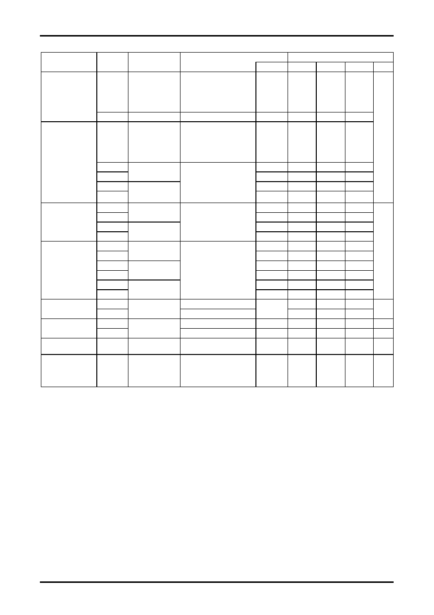
LC88F83B0A
No.A1228-15/25
Electrical Characteristics at Ta = -20°C to +75°C, VSS = LCDVSS0 = LCDVSS1 = 0V
Parameter
Symbol
Pin/Remarks
Conditions
Specification
VDD[V]
min
typ
max
unit
High level input
current
IIH(1)
PORT 0, 1, 2
Output disabled
Pull-up resister OFF
VIN=VDD
(including OFF state leak
current of the output Tr.)
2.7 to 5.5
1
μA
IIH(2)
RESB
VIN=VDD
2.7 to 5.5
1
Low level input
current
IIL(1)
PORT 0, 1, 2
Output disabled
Pull-up resister OFF
VIN=VSS
(including OFF state leak
current of the output Tr.)
2.7 to 5.5
-1
IIL(2)
PORT 0, 1, 2
Output disabled
Pull-up resister ON
VIN=VSS
(including OFF state leak
current of the output Tr.)
4.5 to 5.5
-117
-25
IIL(3)
2.7 to 3.0
-31
-5.8
IIL(4)
RESB
4.5 to 5.5
-10.2
-3.7
IIL(5)
2.7 to 3.0
-6.3
-2.4
High level output
current
IOH(1)
CMOS output mode
PORT0, 2
VOH(1)=VDD-1.0V
4.5 to 5.5
-3.7
mA
IOH(2)
2.7 to 3.0
-1.6
IOH(3)
CMOS output mode
PORT1
4.5 to 5.5
-10
IOH(4)
2.7 to 3.0
-4.5
Low level output
current
IOL(1)
PORT0, 2
VOL(1)=VSS+1.0V
4.5 to 5.5
10
IOL(2)
2.7 to 3.0
4.4
IOL(3)
PORT1
4.5 to 5.5
14.5
IOL(4)
2.7 to 3.0
6.5
IOL(5)
SEG71 to SEG56
4.5 to 5.5
0.5
IOL(6)
2.7 to 3.0
0.5
Common output
current
IOH(5)
COM0 to COM15
VOH(2)=VLCD4-0.05V
2.7 to 5.5
-25
μA
IOL(7)
VOL(2)=VSS+0.05V
25
Segment output
current
IOH(6)
SEG0 to SEG71
VOH(2)=VLCD4-0.05V
2.7 to 5.5
-10
IOL(8)
VOL(2)=VSS+0.05V
10
Hysterisis voltage
VHYS(1)
PORT 0, 1, 2
RESB
2.7 to 5.5
0.1VDD
V
Pin capacitance
CP
All pins
For pins other than that
under test: VIN=VSS
f=1MHz
Ta=25
°C
2.7 to 5.5
10
pF
发布紧急采购,3分钟左右您将得到回复。
相关PDF资料
PIC16F87T-I/ML
IC MCU FLASH 4KX14 EEPROM 28QFN
PIC16F87T-E/ML
IC MCU FLASH 4KX14 EEPROM 28QFN
PIC16F87-E/ML
IC MCU FLASH 4KX14 EEPROM 28QFN
PIC18LF4320-I/ML
IC MCU FLASH 4KX16 EEPROM 44QFN
PIC16F77T-I/PTG
IC MCU FLASH 8KX14 W/AD 44TQFP
PIC16LF1933-I/SO
IC PIC MCU FLASH 4K 28-SOIC
PIC16C54C-20I/SO
IC MCU OTP 512X12 18SOIC
PIC16LF726-I/SO
IC PIC MCU FLASH 8K 1.8V 28-SOIC
相关代理商/技术参数
PIC16F87T-I/ML
功能描述:8位微控制器 -MCU 7KB 368 RAM 16 I/O RoHS:否 制造商:Silicon Labs 核心:8051 处理器系列:C8051F39x 数据总线宽度:8 bit 最大时钟频率:50 MHz 程序存储器大小:16 KB 数据 RAM 大小:1 KB 片上 ADC:Yes 工作电源电压:1.8 V to 3.6 V 工作温度范围:- 40 C to + 105 C 封装 / 箱体:QFN-20 安装风格:SMD/SMT
PIC16F87T-I/SO
功能描述:8位微控制器 -MCU 7KB 368 RAM 16 I/O RoHS:否 制造商:Silicon Labs 核心:8051 处理器系列:C8051F39x 数据总线宽度:8 bit 最大时钟频率:50 MHz 程序存储器大小:16 KB 数据 RAM 大小:1 KB 片上 ADC:Yes 工作电源电压:1.8 V to 3.6 V 工作温度范围:- 40 C to + 105 C 封装 / 箱体:QFN-20 安装风格:SMD/SMT
PIC16F87T-I/SS
功能描述:8位微控制器 -MCU 7KB 368 RAM 16 I/O RoHS:否 制造商:Silicon Labs 核心:8051 处理器系列:C8051F39x 数据总线宽度:8 bit 最大时钟频率:50 MHz 程序存储器大小:16 KB 数据 RAM 大小:1 KB 片上 ADC:Yes 工作电源电压:1.8 V to 3.6 V 工作温度范围:- 40 C to + 105 C 封装 / 箱体:QFN-20 安装风格:SMD/SMT
PIC16F882-E/ML
功能描述:8位微控制器 -MCU 3.5KB Enh FLSH 128 RAM RoHS:否 制造商:Silicon Labs 核心:8051 处理器系列:C8051F39x 数据总线宽度:8 bit 最大时钟频率:50 MHz 程序存储器大小:16 KB 数据 RAM 大小:1 KB 片上 ADC:Yes 工作电源电压:1.8 V to 3.6 V 工作温度范围:- 40 C to + 105 C 封装 / 箱体:QFN-20 安装风格:SMD/SMT
PIC16F882-E/SO
功能描述:8位微控制器 -MCU 3.5KB Enh FLSH 128 RAM RoHS:否 制造商:Silicon Labs 核心:8051 处理器系列:C8051F39x 数据总线宽度:8 bit 最大时钟频率:50 MHz 程序存储器大小:16 KB 数据 RAM 大小:1 KB 片上 ADC:Yes 工作电源电压:1.8 V to 3.6 V 工作温度范围:- 40 C to + 105 C 封装 / 箱体:QFN-20 安装风格:SMD/SMT
PIC16F882-E/SP
功能描述:8位微控制器 -MCU 3.5KB Enh FLSH 128 RAM RoHS:否 制造商:Silicon Labs 核心:8051 处理器系列:C8051F39x 数据总线宽度:8 bit 最大时钟频率:50 MHz 程序存储器大小:16 KB 数据 RAM 大小:1 KB 片上 ADC:Yes 工作电源电压:1.8 V to 3.6 V 工作温度范围:- 40 C to + 105 C 封装 / 箱体:QFN-20 安装风格:SMD/SMT
PIC16F882-E/SS
功能描述:8位微控制器 -MCU 3.5KB Enh FLSH 128 RAM RoHS:否 制造商:Silicon Labs 核心:8051 处理器系列:C8051F39x 数据总线宽度:8 bit 最大时钟频率:50 MHz 程序存储器大小:16 KB 数据 RAM 大小:1 KB 片上 ADC:Yes 工作电源电压:1.8 V to 3.6 V 工作温度范围:- 40 C to + 105 C 封装 / 箱体:QFN-20 安装风格:SMD/SMT
PIC16F882-I/ML
功能描述:8位微控制器 -MCU 3.5KB Enh FLSH 128 RAM RoHS:否 制造商:Silicon Labs 核心:8051 处理器系列:C8051F39x 数据总线宽度:8 bit 最大时钟频率:50 MHz 程序存储器大小:16 KB 数据 RAM 大小:1 KB 片上 ADC:Yes 工作电源电压:1.8 V to 3.6 V 工作温度范围:- 40 C to + 105 C 封装 / 箱体:QFN-20 安装风格:SMD/SMT